Lecture Announcement,
Introductory Quantum Mechanics for Engineers, The course consists of six hours (0.75 CFU), and lectures will be on:
Monday May 23rd , 3 hours
Tuesday May 24th , 3 hours
Denis Rideau
STMicroelectronics TR&D
850 rue Jean Monet, Crolles , France
There is currently a high increase of the market demand for Single Photon Avalanche Diodes (SPAD) for smart phone camera ranging and automotive imaging detection and ranging (LiDAR) applications. Today, most of SPADs in the market are composed of a micrometric semiconductor P-N junction associated to a proximity CMOS electronics biasing the system above the breakdown voltage and quenching the avalanche current after the signal detection.
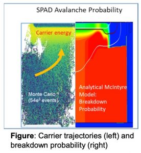
The purpose of this seminar is to provide an overview of the key concepts governing SPAD devices behavior including the coupling with light, the breakdown probability (see figure – right), carrier transport toward the avalanche region (see figure – left), and the impact of the quenching circuit on the device performance. This broad modeling perspective, based on the last 10 years of industrial SPAD developments and characterization at STMicroelectronics, aims to provide to the students a theoretical background for future research in the field.
Seminar Outlook:
- Introduction to SPAD products and market.
- Basics SPAD CMOS circuits.
- The SPAD statistical response: Photon Detection Efficiency (PDE),timing responses to incoming photon (Jitter).
- SPAD hierarchical modelling approach: from Monte Carlo to TCAD.
- Light Absorption: the meta-lenses and meta-surfaces as a path forSPAD performance improvement.
- Semiconductor defects: the Dark Count Rate parasitic noise to solve.

Curriculum Vitae
Denis Rideau received a Ph.D. degree in Physics from the University of Orsay, France in 2001, and an Engineering degree at ESIEE, Paris in 1996. He is now performing TCAD (Technology Computer Aided Design) simulations and advanced modelling at STMicroelectronics, Crolles in France.
His research interests are modelling and simulation of semiconductor nanodevices, with emphasis on quantum effects, strain effects, wafer orientations, and alternative channel materials in FDSOI and FinFets transistors. He is currently working on the design and the modelling of advanced optical sensors and SPAD devices. He has developed several codes for computing the electronic bandstructures and the optical absorption in strain Si, Ge, and SiGe devices using the k.p-Schrödinger, Empirical Pseudo Potential and Tight Binding approaches. In parallel he developed advanced solvers (Monte Carlo and NEGF) to simulate the transport properties of single-gate and multi-gate devices featuring stress, substrate orientation, SiGe materials and high-k/metal gate. He is an expert in the calibration of industrial TCAD softwares aiming in providing physical-grounded parameters but also validation and benchmarking on experimental data. He also investigates by means of TCAD simulations advanced devices, including alternative III-V channel materials and alternative materials and meta-surfaces for optical absorption enhancement.
